Wafer-on-Wafer (WoW) Technology Market, Trends, Business Strategies 2025-2032
Wafer-on-Wafer (WoW) Technology Market was valued at $1.2 billion in 2024 and is projected to reach $4.5 billion by 2032, growing at a CAGR of 15.7 % during the forecast period
Download Sample Report PDF https://semiconductorinsight.com/download-sample-report/?product_id=107972
Executive Summary
The Wafer-on-Wafer (WoW) technology market represents a transformative segment in advanced semiconductor packaging and 3D integration. Valued at $1.2 billion in 2024, the market is on a high-growth trajectory, projected to surge to $4.5 billion by 2032. This expansion, driven by a formidable CAGR of 15.7% during the forecast period (2025-2032), underscores the critical role of WoW in meeting the insatiable demand for higher performance, energy efficiency, and transistor density in applications ranging from AI accelerators and high-performance computing (HPC) to next-generation data centers.
Introduction to Wafer-on-Wafer (WoW) Technology
Wafer-on-Wafer (WoW) technology is an advanced 3D integration technique where fully fabricated semiconductor wafers are directly bonded and interconnected vertically, before being diced into individual chips or chip stacks. Unlike the more common Chip-on-Wafer (CoW) approach, WoW offers superior scalability for mass production of 3D-stacked devices, enabling unprecedented levels of interconnect density and bandwidth while reducing form factor and power consumption. This technology is pivotal in overcoming the limitations of traditional Moore's Law scaling, facilitating the creation of heterogeneous systems that combine logic, memory, and specialty functions in a single, compact package.
Market Size and Growth Forecast (2024-2032)
The market is poised for significant financial growth, driven by the urgent need for advanced packaging solutions.
-
Market Size (2024): USD 1.2 Billion
-
Projected Market Size (2032): USD 4.5 Billion
-
Compound Annual Growth Rate (CAGR 2025-2032): 15.7%
This robust growth is fueled by massive investments in AI infrastructure, the proliferation of 5G/6G networks, and the exponential data processing needs of cloud computing. The transition from monolithic system-on-chips (SoCs) to disaggregated, heterogeneously integrated designs using WoW is a primary market catalyst.
Access the sample report for more details: Download Sample Report PDF
Key Market Trends and Drivers (2025-2032)
-
Dominance of AI and HPC Workloads: The training and inference of large language models (LLMs) require immense memory bandwidth and compute density, making WoW integration of logic and High-Bandwidth Memory (HBM) essential.
-
Advanced Node Scaling Challenges: As transistor shrinkage at leading-edge nodes (e.g., 2nm, 1.4nm) becomes exponentially complex and costly, WoW offers a more economical path to performance gains through "More-than-Moore" 3D integration.
-
Rise of Heterogeneous Integration (HI): There is a strategic shift towards combining specialized chiplets (e.g., CPU, GPU, I/O, RF) from different process nodes into a single package. WoW is a key enabler for high-yield, high-density chiplet integration.
-
Demand for Energy Efficiency: WoW's ultra-short vertical interconnects significantly reduce data transfer distances and power consumption, a critical factor for data center sustainability and mobile devices.
-
Material and Bonding Innovations: Advancements in hybrid bonding (copper-to-copper dielectric bonding) and the exploration of new dielectric materials are enhancing yield, reliability, and interconnect density for WoW stacks.
4. Business Strategies and Competitive Landscape
Leading companies are adopting aggressive strategies to secure leadership in this high-stakes market:
-
Vertical Integration and Partnerships: Foundries and design houses are forming deep alliances (e.g., TSMC with key clients like NVIDIA and AMD) to co-optimize chip design, process technology, and WoW packaging.
-
Heavy R&D Investment: Billions are being allocated to develop next-generation WoW capabilities, such as multi-wafer stacking (>2 layers) and integration of novel materials like silicon photonics.
-
Capacity Expansion: Major players are investing in new advanced packaging facilities (fabs) specifically dedicated to 3D integration technologies, including WoW, to alleviate industry-wide capacity constraints.
-
Intellectual Property (IP) Development: Creating robust portfolios of patents related to bonding techniques, thermal management, and testing methodologies for 3D-stacked wafers is a key strategic focus.
Key Players in the WoW Technology Market
The competitive landscape is dominated by global semiconductor giants with significant technological and manufacturing capabilities.
-
Taiwan Semiconductor Manufacturing Company (TSMC) (Taiwan)
-
NVIDIA Corporation (U.S.)
-
Advanced Micro Devices, Inc. (U.S.)
-
Samsung Electronics Co., Ltd. (South Korea)
-
Intel Corporation (U.S.)
Challenges and Restraints
-
High Manufacturing Complexity and Cost: WoW processes involve extreme precision in alignment, bonding, and thinning, requiring highly specialized and expensive equipment, which impacts overall cost.
-
Yield Management: A single defect can render an entire bonded wafer pair unusable, making yield optimization and sophisticated testing protocols paramount and challenging.
-
Thermal Management: Concentrating immense compute power in a 3D stack creates significant heat flux, requiring innovative cooling solutions (e.g., microfluidic channels, advanced TIMs) that are still in development.
-
Supply Chain and Standards: The ecosystem for WoW is still maturing, with a need for standardized interfaces, testing protocols, and a robust supply chain for materials and equipment.
-
Intellectual Property (IP) Development: Creating robust portfolios of patents related to bonding techniques, thermal management, and testing methodologies for 3D-stacked wafers is a key strategic focus.
5. Key Players in the WoW Technology Market
The competitive landscape is dominated by global semiconductor giants with significant technological and manufacturing capabilities.
-
Taiwan Semiconductor Manufacturing Company (TSMC) (Taiwan)
-
NVIDIA Corporation (U.S.)
-
Advanced Micro Devices, Inc. (U.S.)
-
Samsung Electronics Co., Ltd. (South Korea)
-
Intel Corporation (U.S.)
Download Sample Report PDF https://semiconductorinsight.com/download-sample-report/?product_id=107972
Conclusion and Future Outlook (2032 and Beyond)
The Wafer-on-Wafer technology market is set to become a cornerstone of the semiconductor industry's future. The projected growth to $4.5 billion by 2032 reflects its strategic importance. Beyond 2032, the market is expected to evolve towards more complex, multi-wafer stacks and the integration of quantum computing elements and photonic interconnects within WoW architectures. Success will be determined by overcoming yield and thermal challenges, fostering industry-wide collaboration, and continuous innovation in materials science and process technology. Companies that master WoW integration will hold a decisive advantage in powering the next wave of technological breakthroughs.
Explore Related Outgoing Coverage in semicoductorinsight Domain
https://semiconductorinsight.com/report/radio-access-network-ran-equipment-market/
https://semiconductorinsight.com/report/tunable-rf-inductors-market/
https://semiconductorinsight.com/report/automotive-pcba-board-market/
https://semiconductorinsight.com/report/detuned-reactors-market/
https://semiconductorinsight.com/report/quartz-pressure-sensor-market/
https://semiconductorinsight.com/report/air-variable-capacitor-market/
https://semiconductorinsight.com/report/gallium-nitride-gan-epiwafers-market/
Kategorien
Mehr lesen
NordVPN's Threat Protection Pro Achieves Second AV-Comparatives Certification In a remarkable achievement for cybersecurity tools, NordVPN has once again received certification from independent testing lab AV-Comparatives for its exceptional phishing protection capabilities. The company's Threat Protection Pro feature demonstrated impressive performance by successfully identifying and blocking...
The seamless operation of modern automated systems depends heavily on the precise coordination of multiple processes, where timing accuracy directly influences productivity and system integrity. Components produced by a specialized Time Relay Factory provide the critical timing functions that enable this coordination, serving as the metronome that keeps complex operations in perfect...
Reinventing Horror: Live Theater Takes on the Supernatural In an era dominated by digital effects and screen scares, there's something refreshingly primal about experiencing terror in a shared physical space. The latest theatrical adaptation bearing the name of a well-known horror franchise demonstrates this principle effectively, trading hidden cameras and found footage for the immediate...
"Latest Insights on Executive Summary Nivolumab Market Share and Size CAGR Value The global Nivolumab market was valued at USD 1.71 Billion in 2024 and is expected to reach USD 3.20 Billion by 2032 To produce the best market research report, a wide range of objectives is required to be kept in mind. The large scale Nivolumab Market report is comprehensive and object-oriented which is...
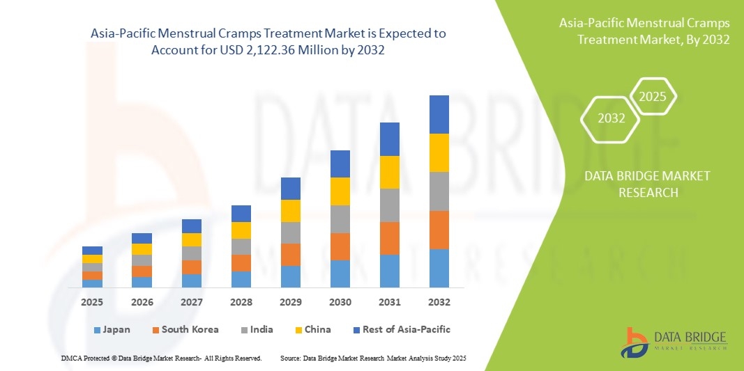
"Executive Summary Asia-Pacific Menstrual Cramps Treatment Market Size, Share, and Competitive Landscape CAGR Value The Asia-Pacific Menstrual Cramps Treatment Market size was valued at USD 1019.38 million in 2024 and is expected to reach USD 2,122.36 Million by 2032, at a CAGR of 9.60% during the forecast period. The market growth is largely driven by the increasing prevalence of...